Fast PCB Prototypes

Latest News
January 6, 2016
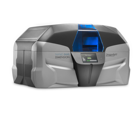
Electronics engineers got an early 3D printing Christmas present. At the Printed Electronics USA conference in November, Nano Dimension demonstrated its three-axis inkjet DragonFly 2020 3D printer, which is designed to build functional, multi-layer circuit board prototypes in just a few hours.
Companies frequently outsource production of printed circuit board (PCB) prototypes because of the time and expense involved in building them. The DragonFly printer could allow them to take those operations in house.
According to the company, the printer can create a complete multi-layer PCB including all interconnections between layers. The device uses conductive nano-inks, and can accept industry standard Gerber design files. Users can test PCBs on the fly. The printer also uses an integrated sintering process to cure the inks, eliminating a number of post-processing steps.
By developing these prototypes internally, designers can spend more time exploring design options while also protecting valuable intellectual property that could be leaked by a third-party prototype contractor.
“For designers and engineers looking for ultra-rapid prototyping of PCBs, our 3D printer is a significant leap forward. The DragonFly 3D Printer eliminates the frustration they face when they reach the prototyping and testing stage,” said Simon Fried, chief marketing officer at Nano Dimension. “Moving their work from design to a prototype at an off-site printing facility might take weeks for the PCB to be ordered, produced and shipped. If further iterations are needed, it’s back to the prototyping house for another cycle. In today’s competitive electronics markets, unforeseeable and costly delays during PCB development can significantly slow time-to-market. That’s the development risk and bottleneck that we’re eliminating with the DragonFly 2020.”
The initial model has a print envelop of 20cm by 20cm, but larger versions are in development. The company developed its AgCite conductive silver nanoparticle inks with Yissum, a Hebrew University tech transfer company.
The inks are available now; the printer will be released in 2016.
In November, the company also filed a patent for a copper ink. You can learn more about the printers in the video below.
Source: Nano Dimension
Subscribe to our FREE magazine, FREE email newsletters or both!
Latest News
About the Author
Brian Albright is the editorial director of Digital Engineering. Contact him at [email protected].
Follow DE

